Integrating Virtual Memory in ARA a RISC-V Vector Coprocessor: A Milestone for Linux Compatibility and High-Performance Computing
Virtual memory is essential for modern processor design, providing benefits like memory protection, efficient multitasking, and abstraction of physical memory management. It allows systems to handle larger applications and improve security by isolating processes.
Many open-source RISC-V vector processors, such as ARA from the PULP platform, lacked virtual memory support, which limited their ability to handle complex, memory-heavy applications. Since ARA operated in bare-metal mode, it couldn’t boot Linux or manage advanced multitasking. Recent efforts have focused on adding virtual memory by sharing the MMU of the Ariane core currently known as OpenHW CVA6. This improvement enables ARA to run more complex vector applications and enhances its performance in demanding computing tasks.
Introduction of Ara and CVA6
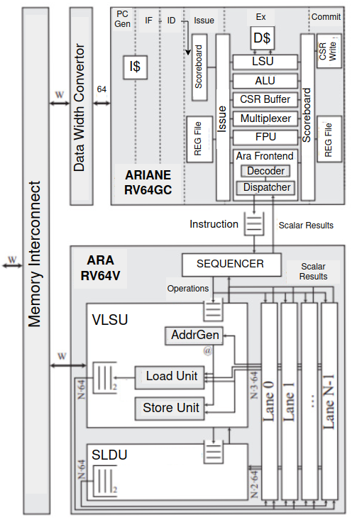
ARA is a high-performance 64-bit vector unit designed by the PULP platform, fully compliant with the RISC-V Vector 1.0 Extension for data-parallel applications [1] [2]. Developed as a co-processor of CVA6, it enhances workloads by performing operations on multiple data elements simultaneously. ARA supports mixed-precision arithmetic, optimizing both speed and energy efficiency. Its architecture includes several components like the Vector Load/Store Unit (VLSU), slide unit, and lanes that collaborate to execute vector instructions effectively. The integration with the CVA6 core is facilitated through the first pass decoder, ensuring efficient instruction routing.
ARA’s dispatcher manages the interface between ARA and CVA6’s instruction issue stage, while ARA sequencer tracks instruction progress, dispatching them to various execution units like the ALU, FPU, and multiplier. The VLSU manages memory operations by interfacing with the AXI4 bus, handling data transfers between memory and the vector register file. ARA is scalable, supporting up to four independent lanes, each with a VLEN of 1024, allowing parallel execution of vector instructions. Its modular design balances performance and resource utilization, with support for unit-strided, strided, and indexed memory access patterns, ensuring efficient data transfers.
CVA6, also known as Ariane, is a 64-bit application-class RISC-V core developed by the pulp team, featuring a six-stage pipeline and designed for high-performance computing tasks [3]. It supports multiply/divide, atomic operations, and an IEEE-compliant FPU, and is compatible with booting Linux. Ariane acts as a wrapper for CVA6, allowing the integration of extensions and co-processors like ARA. ARA is integrated into the execution stage of CVA6, where vector instructions are partially decoded and sent to ARA through a first-pass decoder. The six pipeline stages include instruction fetch, decode, issue, execution, and commit, with the backend supporting co-processor integration.
Selected configurations of ARA and CVA6
To optimize performance and resource utilization within the development environment, the ARA vector coprocessor was configured with 2 lanes and a vector length (VLEN) of 512 bits. This setup provides parallelism for vector operations while staying within the constraints of FPGA resources. The 512-bit VLEN ensures sufficient data width for typical vector tasks, balancing performance with resource efficiency. On the Ariane side, the Floating Point Unit (FPU) and Bit Manipulation extension were disabled to reduce the logic footprint and conserve FPGA resources. These decisions streamlined the design, focusing on integer-based vector operations and efficient memory management.
ARA as a submodule of Ariane
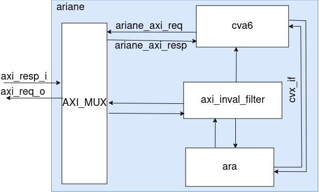
The ARA is integrated with the CVA6 core in a SOC called ara_soc, where both ARA and Ariane are connected in parallel. However, ara_soc has a key limitation—it does not support Ariane’s capability to boot Linux, restricting its use for full operating system testing. To overcome this, the Ariane environment, which fully supports Linux booting and a wide range of peripherals, is used for more comprehensive testing and development. In this environment, ARA is instantiated as a submodule of CVA6 and ARA is integrated with CVA6 within the Ariane wrapper using the CVXIF port and key components to manage data flow and ensure cache coherence. This integration includes an invalidation filter and an AXI multiplexer. The invalidation filter maintains cache coherence by detecting when ARA’s performs a memory operation which affects the cache of CVA6, generating invalidation requests to keep data consistent across both cores. The AXI multiplexer directs and multiplexes AXI requests between ARA and CVA6, ensuring efficient data routing.
CVA6’s Modifications
The design approach includes sharing the Ariane’s Memory Management Unit (MMU) with ARA. To create a communication path from ARA’s Vector Load/Store Unit (VLSU) to the MMU, additional signals are incorporated into the CVXIF port.
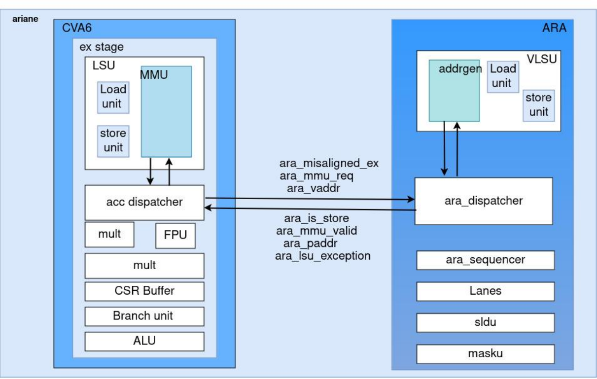
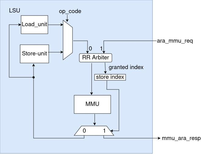
In order to share the MMU with Ara, a round-robin arbiter is implemented within this process, with an additional port introduced in the LSU specifically for handling ARA’s translation requests. Round Robin arbiter is used to ensure the fairness and systematic approach to access the shared TLBs of MMU. Requests from the vector and scalar units are fed into the arbiter through a 2-bit input, with scalar requests assigned to index zero and vector requests to index one. The arbiter grants one request at a time, registering the index of the granted request and forwarding it to the MMU.
ARA’s Modifications
A key decision in the redesign process was determining where to integrate the MMU interface within the AGU. Two main options were considered: modifying the Address Generator FSM or altering the AXI Request Generation FSM. After careful consideration, it was determined that the latter would be the optimal choice, as it is responsible for forwarding addresses to the AXI channels. Consequently, the AXI Request Generation FSM was redesigned to accommodate an additional port with the MMU.
An additional state of AXI_ADDRGEN_WAIT_MMU is added to the existing FSM. The primary concept involves sending the base address for translation in both unit-strided and strided operations. The AXI request aligns with 4KiB pages. The boundaries of the current page and the next page are calculated and stored. So, If a transaction crosses a page boundary, a new request is sent to the MMU with the next 4KiB page base address for translation. Counters are used to add the offset based on stride in each cycle, monitoring the transaction length. When the transaction length reaches zero, the operation ends.
For indexed operations, a translation request must be sent to the MMU for each transaction because the index value cannot be determined without reading it from the VRF. To minimize the latency of waiting for the MMU, the next address is read from spill registers and sent to the MMU simultaneously, while the physical address is sent on the AXI channel in parallel. This process eliminates a cycle wait for each transaction under ideal conditions (TLB hit).
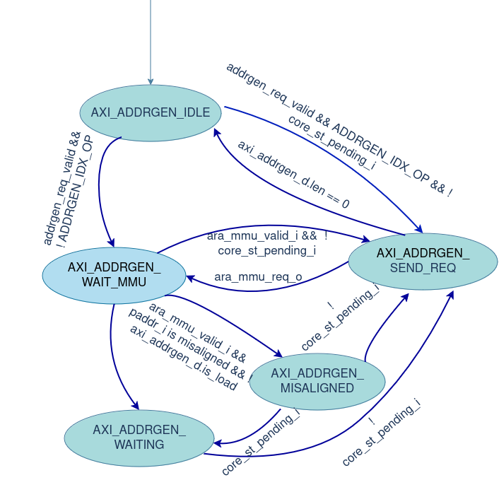
The FSM starts in the AXI_ADDRGEN_IDLE state, where it waits for a memory request from the Address Generation FSM. Once a request is received, indicating the need to access memory, the FSM forwards the virtual base address to the MMU for translation.
In the AXI_ADDRGEN_WAIT_MMU state, the FSM waits until the MMU returns the corresponding physical address.
If the physical address is properly aligned, the FSM transitions to the AXI_ADDRGEN_SEND_REQ state. In this state, it generates sequential memory addresses, handling unit-strided or custom-strided operations. The FSM monitors page boundaries (aligned to 4KiB) to avoid crossing into a new page without requesting a new base address from the MMU. If a boundary is crossed, it returns to the AXI_ADDRGEN_WAIT_MMU state for further address translation.
If the address from the MMU is misaligned, the FSM moves to the AXI_ADDRGEN_MISSALIGNED state to handle the adjustment and ensure correct data access.
In the AXI_ADDRGEN_WAITING state, the FSM stalls if there is a pending store in the store buffer, ensuring memory coherence. For indexed operations, the FSM skips the IDLE state and directly transitions to the AXI_ADDRGEN_WAIT_MMU state to request a physical address from the MMU, using the virtual address from the spill registers, while simultaneously sending the current physical address to the AXI channel.
Verification Efforts
The vector memory tests verify the vector core’s ability to handle memory accesses in user mode, focusing on translating virtual addresses to physical addresses. After setting up Page Table Entries (PTEs), reference data is generated using the vid.v instruction, which initializes the vector register with a predictable sequence. The tests then switch to user mode to perform unit-strided, strided, and indexed operations.
For load operations, scalar store operations save modified reference data into memory at offsets based on the Selected Element Width (SEW): 1 byte for SEW = 8, 2 bytes for SEW = 16, 4 bytes for SEW = 32, and 8 bytes for SEW = 64. After data is stored, the vector load operation retrieves data into the vector register file, and vmsne.vv and vpopc.m instructions compare the loaded data to the reference data to check for discrepancies.
For store operations, a vector store writes data from the vector register into memory sequentially. The stored data is then retrieved via scalar load operations for comparison against the reference data. Discrepancies between the loaded and reference data highlight potential issues with store operations. The process ensures the correctness of unit-strided, strided, and indexed vector memory operations across different SEWs.
A customized, self-checking algorithm was developed to efficiently manage load and store operations on large data chunks in a virtual memory environment, simulating real-world application scenarios. Initially implemented using scalar instructions, the algorithm processed one data element per cycle, testing memory management and address translation in user mode with virtual memory enabled. However, this scalar approach was inefficient for large datasets due to its lack of data-level parallelism, resulting in longer execution times.
To overcome this, the algorithm was re-implemented using vector instructions, allowing multiple data elements to be processed simultaneously, significantly improving throughput and efficiency. The vectorized version, also tested in user mode with virtual memory, demonstrated superior performance, making it ideal for handling extensive data operations. The pseudocode of the algorithm is shown below.
					// Generate ELNUM bytes of data
data = generate_data(ELNUM)

// Store data at address A and address B
memory[A] = data
memory[B] = data

// Load data from address A and address B into registers X and Y respectively
X = load(memory[A])
Y = load(memory[B])

// Multiply values in registers X and Y
result = multiply(X, Y)

// Store the result at address C
memory[C] = result

// Load data from address C into registers X and Y
X = load(memory[C])
Y = load(memory[C])

// Compare values in registers X and Y
if compare(X, Y):
	// If X and Y are equal, continue with next operations
	// Further operations can be defined based on requirements
	pass
else:
	fail
Conclusion
This project successfully enabled virtual memory support for the ARA vector coprocessor, a key step toward running Linux and vector-based applications. While fully booting Linux on ARA was hindered by the limited capacity of available FPGA platforms, testing on these platforms validated the design. This work demonstrates the feasibility of virtual memory integration in open-source vector processors like ARA, paving the way for future enhancements and broader use in high-performance computing. Future efforts will focus on scaling TLB implementations to fully exploit ARA’s virtual memory capabilities.
Bibliography
[1] Cavalcante, M., Schuiki, F., Zaruba, F., Schaffner, M., & Benini, L. (2021). Ara: A Scalable and Energy-Efficient RISC-V Vector Processor with Multi-Precision Floating Point Support in 22 nm FD-SOI. IEEE Transactions on Computers, 70(7), 1173-1187
[2] “Working draft of the proposed RISC-V V vector extension,” 2019, accessed on March 1, 2023. [Online]. Available: https://github.com/riscv/riscv-v-spec
[3] Zhang, Y., Gu, Y., & Zhang, W. (2020). Design and Implementation of CVA6: A High-Performance RISC-V CPU Core for Embedded Applications. Journal of Systems Architecture, 107(1), 101725.